
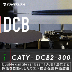
Automated wafer bonding strength evaluation device using the DCB method.
Contributing to the evaluation of the wafer bonding process!
In the advancement of high-performance advanced semiconductor devices, 3D integration has become essential. Plasma-activated direct bonding is used for the joining of wafers. The processes after bonding often impose loads on the bonding surface, making the management and measurement of bonding strength crucial. The DCB device has been designed and developed as a dedicated machine for evaluating the direct bonding strength of wafers. ◆ Quantification of bonding strength evaluation using a double cantilever beam ◆ ◆ High-precision analysis of Si wafer bonding strength, quantifying reliability from surface energy ◆ The formula treating surface energy as bonding strength was introduced by WP. Maszara and can be derived from the formula on the left. E [GPa] is the Young's modulus of the Si wafer, t_b [mm] is the thickness of the blade, t_w [mm] is the thickness of one wafer, L [mm] is the delamination distance. *This device has been manufactured under the supervision of Professor Fumihiro Inoue from Yokohama National University. ◆ Equipped with features that allow for easy operation even within a glove box ◆ ◆ Capable of imaging delamination distance with a high-quality SWIR camera and uniform NIR LED lighting ◆ ◆ [Introduction to the bondwave device] Visualizing the plasma bonding process with NIR ◆
- Company:米倉製作所
- Price:Other
